Semiconductor Manufacturing Equipment Market Growth Report, 2026-2034
REPORT DETAILS
Market Statistics
Market Overview
The global semiconductor manufacturing equipment market size was valued at USD 109.33 billion in 2025. The semiconductor manufacturing equipment market CAGR is projected to be 7.6% during 2026–2034. The market is driven by the growing demand for advanced electronics and 5G technology, the increasing adoption of automation and sustainability strategies, and the geopolitical forces that create a need for local manufacturing. The market is also fueled by substantial government investments to enhance local semiconductor development.
The semiconductor manufacturing equipment market comprises equipment used to make and assemble chips. This encompasses wafer fabrication equipment (WFE) used in initial production stages, such as patterning, layering, cleaning, and polishing, as well as equipment used in later stages for assembling, packaging, cutting, bonding, and testing chips. The demand is increasing due to advanced packaging and chiplet architectures, which require more accurate bonding and high-performance testing equipment.
Key Insights
- The logic segment held the largest market share in 2025. The market dominance is attributed to the need for high-performance computing, AI, and data centers.
- 2D ICs accounted for the largest market share by dimension in 2025. This is attributed to the maturity of the fabrication process, cost-effectiveness, and a well-established ecosystem.
- The Asia Pacific region led the semiconductor manufacturing equipment market in 2025. The well-established semiconductor supply chain and advanced manufacturing capabilities in countries such as Taiwan, South Korea, Japan, and China are responsible for the leading market position.
- North America is expected to have the highest CAGR. The market in North America is fueled by the CHIPS Act, domestic fab construction, and advancements in AI and EUV lithography.
These trends show that semiconductor manufacturers are adopting more advanced and specialized equipment as they move towards smaller and more powerful designs. This includes the increasing adoption of EUV lithography, etch, and inspection tools. On the other hand, investment in advanced packaging tools is also increasing in the dominant semiconductor manufacturing regions.
Industry Dynamics
- The growing demand for 5G and AI technologies requires advanced chips, thereby accelerating investments in high-precision manufacturing equipment.
- The growth of smart manufacturing and automation improves production efficiency. This increases the adoption of advanced semiconductor fabrication equipment.
- Government incentives and subsidies for the domestic production of chips are encouraging investments in new equipment for semiconductor fabrication.
- Increasing R&D investments in advanced packaging and lithography technologies are fueling innovation in the semiconductor manufacturing equipment market.
- High capital expenditure and equipment ordering cycle times make it difficult for smaller semiconductor manufacturers to be flexible.
Market Statistics
2025 Market Size: USD 109.33 billion
2034 Projected Market Size: USD 211.29 billion
CAGR (2026–2034): 7.6%
Asia Pacific: Largest market in 2025
Source: Polaris Market Research Analysis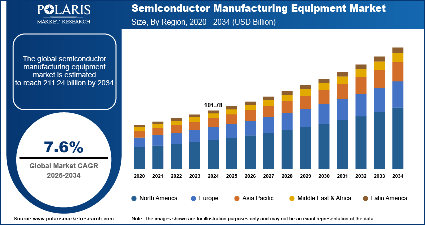
To Understand More About this Research:Download Sample Report
AI Impact on Semiconductor Manufacturing Equipment Market
- The demand for advanced semiconductor manufacturing equipment has increased as AI technology requires more advanced equipment to produce high-performance, energy-efficient chips.
- The automated semiconductor fabrication processes are supported by AI technology, which results in faster production times and improved accuracy and operational efficiency.
- The creation of AI-specific chips requires manufacturers to develop both fresh production equipment and specialized production procedures.
- AI technology helps research and development work by improving both chip design and fabrication methods.
- Semiconductor equipment manufacturers use AI technology to improve machine accuracy while decreasing manufacturing mistakes.
In semiconductor manufacturing, AI is now integrated into measurement and inspection equipment to improve defect detection and accelerate root-cause diagnosis. The semiconductor equipment manufacturer is also applying AI to predictive maintenance, helping factories extend equipment lifespans, prevent unexpected failures, and better manage spare parts. This is particularly important because equipment delivery times are still long, and semiconductor factories want to operate equipment at high utilization rates.
The semiconductor manufacturing equipment market includes equipment, tools, and systems utilized in the manufacturing of semiconductor devices such as integrated circuits (ICs), semiconductor memory chips, and other active electronic components. The semiconductor market is very important to the overall semiconductor industry, which drives technology innovation in industries such as consumer electronics, automotive, telecommunication, and healthcare. The growing use of 5G networks and high-performance computing drives the need for more advanced semiconductor chips, thereby fueling the use of advanced equipment in manufacturing. According to 5G Americas, the number of global 5G connections is expected to reach 6.8 billion by 2027, with North America at 36%, amounting to 601 million connections. This is fueling spending on wafer fabrication equipment (WFE), especially EUV lithography equipment used to produce advanced chips. Chip makers are also spending on deposition and etching equipment to support more complex chip designs, as well as on inspection and measurement equipment to support quality with smaller, more accurate chip features.
Rise in interest in automation and smart manufacturing processes improves productivity and accuracy in semiconductor fabrication facilities, thus fueling the growth of the semiconductor manufacturing equipment market. Moreover, the global movement towards sustainability and energy-efficient technologies helps in the evolution of next-generation semiconductors, thus driving the growth of innovative manufacturing equipment. The current global shifts in geopolitics have led to a surge in semiconductor manufacturing reshoring.
Market Dynamics
Rising Demand for Advanced Electronics
There has been a growing requirement for advanced electronics, including smartphones, IoT, and AI solutions. The need for high-performance, miniaturized electronics has driven substantial investments in modern fabrication technologies such as extreme ultraviolet (EUV) lithography and advanced packaging. The rising demand is fueling innovation in the semiconductor ecosystem and shaping the market dynamics by requiring faster and higher yields. In addition, the adoption of new-age technologies like autonomous vehicles, smart homes, and industrial automation is expanding the semiconductor application space, resulting in an increased requirement for advanced fabrication solutions to cater to the needs of the new technology era.
In terms of equipment, the trend towards smaller, more advanced chips requires more accurate lithography, controlled etching, thin-film deposition, and better process control. The shrinking size of chip features, along with rising quality standards, makes measurement and inspection equipment essential for detecting even the smallest defects.
Increasing Government Initiatives and Funding to Boost Domestic Semiconductor Production
Government initiatives and investments to promote local semiconductor manufacturing in regions such as North America, Europe, and Asia Pacific are creating increasing demand for semiconductor manufacturing equipment. In November 2024, CHIPS for America invested up to USD 300 million in advanced packaging research projects in Georgia, California, and Arizona to accelerate semiconductor development. Strategic investments, including subsidies, tax breaks, and national semiconductor initiatives, are planned to minimize supply chain risks. These policies enable the development of advanced fabrication facilities and promote public-private partnerships that fuel innovation. In addition, government-backed initiatives accelerate research and development activities in next-generation semiconductor materials and manufacturing technology, thus ensuring regional competitiveness and the long-term sustainability of the global semiconductor ecosystem.
Government incentives are also accelerating the start of construction of new chip wafer fabrication facilities. This is also driving demand for front-end equipment, such as lithography, deposition, etching, and polishing, as well as facility systems, including automation, gas management, and chemical distribution. But the actual equipment buying may experience delays due to long equipment delivery times, testing and approval procedures, and installation capacity constraints, which could slow revenue growth even as new fabs are announced.
Fab Process Map & Equipment Categories
The process of semiconductor manufacturing requires structured methods for production. The process needs specific wafer fabrication equipment for each of its stages. The process begins with front-end semiconductor equipment. It enables the creation of tiny circuit patterns on a silicon wafer through layer-by-layer development. The process establishes essential attributes that determine the chip's operating efficiency, power needs, and physical dimensions. The production facility spends most of its budget on front-end semiconductor equipment. The procedure advances to its back-end stage after the fundamental structures have been developed. The process establishes electrical connections between different circuit components.
Semiconductor process control equipment performs ongoing inspections and defect testing of wafers throughout all operational stages. The manufacturing process now requires semiconductor process control equipment because modern chips have become more intricate which results in higher production waste. Advanced packaging equipment assembles chips after their fabrication process ends particularly for high-performance chip production. The semiconductor test equipment assesses chip functionality and reliability before delivery to customers.
CAPEX Cycle, Lead Times & Constraints
The semiconductor manufacturing equipment market operates according to the CAPEX cycle that governs semiconductor industry expenditures. Companies increase their equipment spending during periods of high chip demand because they require additional capacity and technological improvements. This operational period, known as an upcycle, leads to increased orders for wafer fabrication equipment. The downcycle begins when companies cut spending as demand declines and inventory levels rise.
Market conditions depend on the lead time for semiconductor equipment deliveries. The delivery schedule requires several months because most equipment needs custom solutions to address its complex design. The equipment needs to go through a qualification process that ensures its performance remains stable throughout the fab environment. The equipment qualification process takes several months to complete, making equipment planning an extended-timeframe activity. Strong demand periods lead to extended time-cycle delays because component shortages and production capacity issues create constraints.
Source: Polaris Market Research Analysis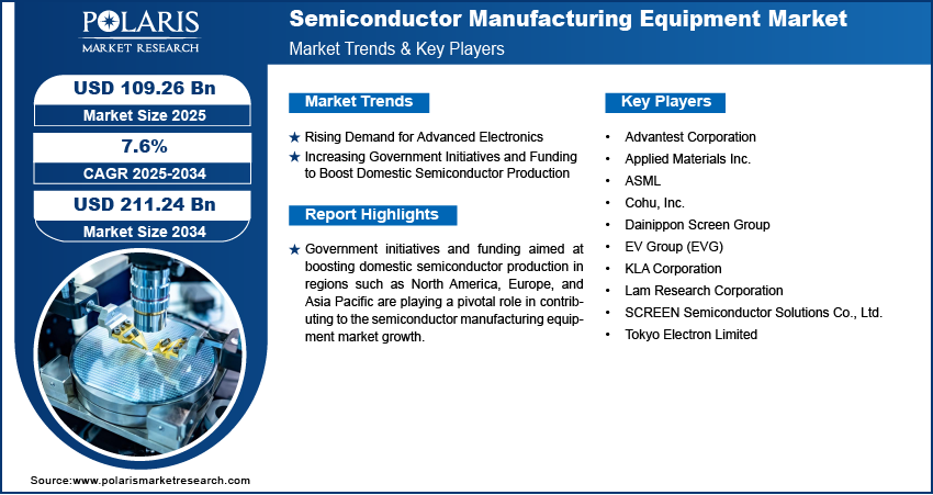
Get Full Segment-Level Forecasts & Insights: Download Sample Report
Segment Insights
Market Assessment by Product Type
The global market segmentation, based on product type, includes memory, MPU, foundry, logic, discrete, and others. In 2025, the logic segment accounted for the largest share of the semiconductor manufacturing equipment market due to the growing demand for high-performance computing, artificial intelligence, and advanced data center operations. Logic chips are critical in the execution of complex tasks. The logic chips are witnessing rapid adoption in various sectors, including automotive electronics, edge computing, and next-generation networking. The increasing complexity of logic chip architectures, such as the move to sub-5nm technology nodes and the integration of heterogeneous systems, is driving investment in advanced lithography, metrology, and inspection tools. This is a reflection of the importance of semiconductor manufacturing in determining the future of digital infrastructure. As logic design transitions to gate-all-around (GAA) architectures and scaled technology nodes, EUV lithography systems will play an essential role in the precise patterning of nanoscale features. Advanced inspection and measurement systems will become even more vital in maintaining production quality and volume.
The memory segment is anticipated to register the highest CAGR during the forecast period. This is due to the rapid growth of data-centric applications and the rising need for high-capacity and energy-efficient memory solutions. AI training applications, real-time analytics, and the growing adoption of cloud computing infrastructure are driving the demand for DRAM and NAND flash. Furthermore, the development of next-generation memory technologies such as MRAM and ReRAM demands advanced manufacturing processes, thereby fueling innovation in equipment. These factors are increasing the emphasis on process improvements and yield optimization in memory fabrication. When memory suppliers increase their production, it is generally accompanied by an increase in the demand for deposition, etching, and cleaning tools, as well as inspection systems used to check for defects in mass production. As suppliers adopt next-generation memory technology, they increasingly turn to advanced measurement tools to improve production yield.
Market Evaluation by Dimension
The global semiconductor manufacturing equipment market segmentation, based on dimension, includes 2D ICs, 2.5D ICs, and 3D ICs. In 2025, the 2D ICs segment had the largest share due to the maturity of traditional fabrication technology. 2D ICs remain the leading technology for high-volume manufacturing across consumer electronics, automotive, and industrial applications because of their well-proven performance and scalability at competitive prices. The well-established ecosystem for 2D IC manufacturing, including equipment manufacturers, foundries, and material suppliers, sustains 2D ICs' market leadership despite growing interest in more advanced integration schemes. The dominance of 2D ICs also supports demand for mature-node wafer fabrication equipment. In these segments, equipment shipments are driven by equipment replacement, capacity expansion, and process enhancements, driven by high equipment utilization.
The 3D ICs segment is expected to register the highest CAGR during the forecast period, driven by the growing need for high-performance, low-power, and small semiconductor solutions. The recent breakthroughs in packaging technology, including through-silicon vias (TSVs) and hybrid bonding, are making it possible to stack multiple dies vertically, thus increasing bandwidth and lowering latency. These needs are critical for AI accelerators, high-end mobile technology, and advanced automotive solutions, which are nearing the end of the road in terms of scaling. The growing investment in R&D related to heterogeneous integration and system-in-package (SiP) technology is fueling the adoption of 3D ICs. This is disrupting the manufacturing model and pushing equipment to the technological frontier.
Source: Polaris Market Research Analysis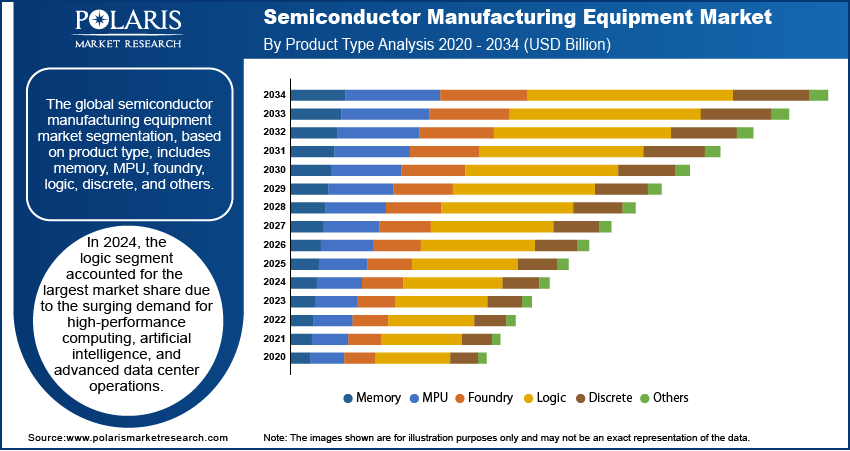
Need Granular Data Across All Market Segments? Request Customization
Regional Outlook
By region, the study provides market insights into North America, Europe, Asia Pacific, Latin America, and the Middle East & Africa. In 2025, Asia Pacific semiconductor manufacturing equipment market held the largest market share due to a comprehensive, vertically integrated semiconductor value chain led by countries such as Taiwan, South Korea, Japan, and China. According to the US International Trade Commission, Taiwan currently accounts for 18% of the world’s semiconductor manufacturing capacity and is home to 92% of the world’s advanced semiconductor manufacturing. Aggressive capital spending by the world’s leading foundries and integrated device manufacturers (IDMs) in next-generation semiconductor fabrication facilities, such as sub-5nm and gate-all-around (GAA) node technologies, is further cementing the region’s position at the top. The Asia Pacific region ascends to the top position in global semiconductor manufacturing due to its strong government-led semiconductor self-reliance programs and advanced lithography, etching, and metrology technologies. The region experiences increased demand for advanced manufacturing equipment due to its vital role in consumer electronics and electric vehicle markets. The region also has a robust local supplier network that provides lithography components, etching, deposition equipment, and inspection and measurement systems. This established supply chain allows the region to support high-volume chip manufacturing and advanced manufacturing processes.
The North America semiconductor manufacturing equipment market is expected to see the highest CAGR over the forecast period due to extraordinary national efforts to enhance the region’s semiconductor manufacturing capabilities. Strategic laws, such as the CHIPS and Science Act, are injecting billions of dollars into the development of advanced fabs, which will drive the demand for advanced equipment. Major tech firms are increasing their domestic manufacturing capabilities. They are focusing on key applications such as AI accelerators, quantum computing, and next-generation communication systems. The push for a secure supply chain, along with advancements in EUV lithography and innovation in processes, is expected to drive the market in North America. Apart from new fab construction, North America’s growth is also driven by rising investments in advanced packaging, process control, and AI-based manufacturing systems. This is creating a need for inspection and measurement tools, factory automation solutions, and advanced lithography systems.
Source: Polaris Market Research Analysis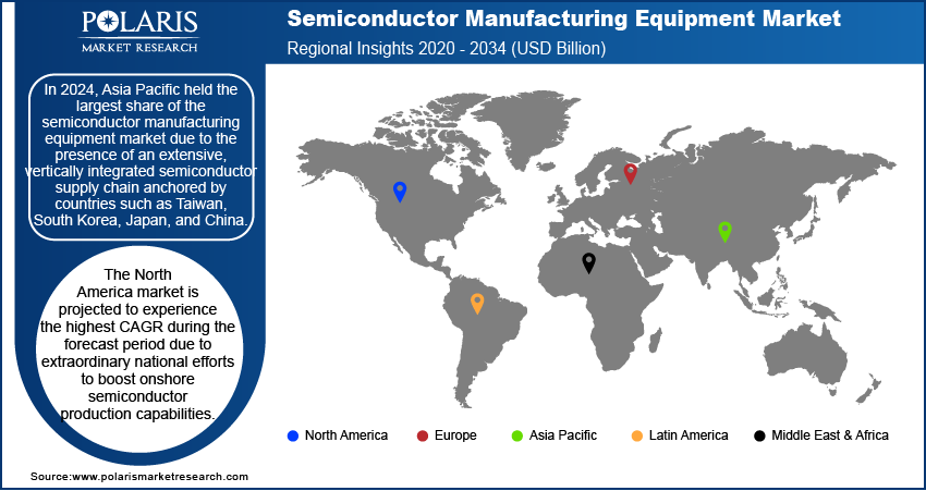
Curious About Regional Market Performance? Request Customization
Key Players and Competitive Analysis
The semiconductor manufacturing equipment market is becoming increasingly competitive, driven by in-depth analysis and expansion strategies. Additionally, the number of strategic alliances being formed in the industry to boost technological strength is increasing. The focus of semiconductor manufacturing equipment firms post-mergers and acquisitions is shifting toward integration. This is because of the need to leverage expertise in areas such as EUV lithography and wafer inspection. The number of product launches in the semiconductor manufacturing equipment industry is increasing, driven by the need to leverage customization in areas such as 3D ICs and heterogeneous integration.
The competitive positioning in the semiconductor manufacturing equipment market is being driven more and more by leadership in certain categories of tools. For instance, ASML is the leader in the advanced EUV lithography systems category, while Applied Materials and Lam Research are strong competitors in the deposition and etching tools category. KLA is a major player in the inspection and measurement systems category, and Advantest and Cohu are well-positioned in the semiconductor testing and handling solutions category. This segmentation is important because, as semiconductors advance to more complex geometries and move towards 3D integration, the need for process control, packaging, and testing continues to escalate.
Technology advancements in fields such as AI-driven metrology, atomic layer deposition, and defect detection are redefining competitive advantages. Partnerships for strategic development with fab operators and material suppliers are further driving the development cycles. They are enabling the quick implementation of next-generation manufacturing solutions. Increased investment in R&D and supply chain collaborations are essential for maintaining a leadership position in the market. The emphasis on sustainability, yield, and cost is further shaping equipment development.
Advantest Corporation offers automatic test equipment (ATE) and measurement equipment used in semiconductor and electronic system testing. The company offers test systems for evaluating system-on-chip (SoC) devices, memory components, and radio frequency (RF) semiconductors. It also provides metrology and inspection solutions such as multi-vision metrology, scanning electron microscopes, and 3D imaging analysis. Advantest provides a broad spectrum of services such as consulting, engineering services, test program development, production ramp-up support, and remote support. The customized production services provided by Advantest can be integrated with the customers’ manufacturing execution systems to enhance efficiency and quality. Advantest operates in 18 countries and has a strong presence in North America, Europe, and Asia. The company has subsidiaries and regional headquarters in major locations such as San Jose, California, and a strong presence in Japan and other major semiconductor markets.
Applied Materials Inc. is a player in the semiconductor manufacturing equipment market. It focuses its efforts on providing equipment, services, and software solutions for the production of integrated circuits, flat panel displays, and solar photovoltaic products. The product line of the company is broad, including tools for thin film deposition, etching, chemical and physical vapor deposition (CVD, PVD), atomic layer deposition (ALD), ion implantation, inspection, metrology, and automation solutions that help in the manufacture of advanced chips and displays at near-atomic levels. Applied Materials also offers software solutions for process optimization and predictive analytics. It also has full-service customer support and consulting. The company is headquartered in Santa Clara, California, and operates globally. It has a strong presence in North America and regional offices in Singapore and Europe.
List of Key Companies
- Advantest Corporation
- Applied Materials Inc.
- ASML
- Cohu, Inc.
- Dainippon Screen Group
- EV Group (EVG)
- KLA Corporation
- Lam Research Corporation
- SCREEN Semiconductor Solutions Co., Ltd.
- Tokyo Electron Limited
Semiconductor Manufacturing Equipment Industry Developments
October 2025: Applied Materials, Inc. (US) launched the Kinex Bonding System, the industry’s first integrated die-to-wafer hybrid bonder, combining die placement, interconnect, and bonding in one platform for high-performance, low-power logic and memory devices.
September 2025: ASML led a major Series C funding round for Mistral AI and formed a long-term partnership to apply Mistral’s AI models across ASML’s R&D, operations, and product performance, while joining Mistral’s strategic committee.
March 2025: US-based Yield Engineering Systems (YES) shipped its first commercial VeroTherm Formic Acid Reflow tool to a major global semiconductor manufacturer. YES produces process equipment for AI and high-performance computing chips from its manufacturing facility.
January 2025: KASFAB Tools opened the first manufacturing and assembly facility in India. The facility is focused on semiconductor equipment and is designed to meet the requirements of global customers. The facility is expected to improve semiconductor manufacturing in India by providing the advanced tools and infrastructure required by the expanding global semiconductor industry.
June 2024: Imec, a nanoelectronics company, and ASML, a lithography equipment supplier, opened the High NA EUV Lithography Lab in Veldhoven, the Netherlands. The facility will be operated jointly by both companies.
Semiconductor Manufacturing Equipment Market Segmentation
By Product Type Outlook (Revenue – USD Billion, 2021–2034)
- Memory
- MPU
- Foundry
- Logic
- Discrete
- Others
By Front-End Equipment Outlook (Revenue – USD Billion, 2021–2034)
- Lithography
- DUV
- EUV
- Wafer Surface Conditioning Equipment
- Etching
- Chemical Mechanical Planarization
- Deposition
- PVD
- CVD
- Cleaning Process
- Single-Wafer Spray System
- Single-Wafer Cryogenic System
- Batch Immersion Cleaning System
- Batch Spray Cleaning System
- Scrubber
- Other Equipment
By Fab Facility Equipment Outlook (Revenue – USD Billion, 2021–2034)
- Automation
- Chemical Control Equipment
- Gas Control Equipment
- Others
By Back-End Equipment Outlook (Revenue – USD Billion, 2021–2034)
- Back-End Processes
- Assembly and Packaging
- Dicing Equipment
- Bonding Equipment
- Metrology Equipment
- Test Equipment
By Dimension Outlook (Revenue – USD Billion, 2021–2034)
- 2D ICs
- 2.5D ICs
- 3D ICs
By Supply Chain Process Outlook (Revenue – USD Billion, 2021–2034)
- IDM Firms
- OSAT Companies
- Foundries
By Regional Outlook (Revenue, USD Billion, 2021–2034)
- North America
- US
- Canada
- Europe
- Germany
- France
- UK
- Italy
- Spain
- Netherlands
- Russia
- Rest of Europe
- Asia Pacific
- China
- Japan
- India
- Malaysia
- South Korea
- Indonesia
- Australia
- Vietnam
- Rest of Asia Pacific
- Middle East & Africa
- Saudi Arabia
- UAE
- Israel
- South Africa
- Rest of Middle East & Africa
- Latin America
- Mexico
- Brazil
- Argentina
- Rest of Latin America
Semiconductor Manufacturing Equipment Market Report Scope
| Report Attributes | Details |
| Market Size in 2025 | USD 109.33 billion |
| Market Size in 2026 | USD 117.47 billion |
| Revenue Forecast by 2034 | USD 211.29 billion |
| CAGR | 7.6% |
| Base Year | 2025 |
| Historical Data | 2021–2024 |
| Forecast Period | 2026–2034 |
| Quantitative Units | Revenue in USD billion, and CAGR from 2026 to 2034 |
| Report Coverage | Revenue Forecast, Market Competitive Landscape, Growth Factors, and Trends |
| Segments Covered |
|
| Regional Scope |
|
| Competitive Landscape | Semiconductor Manufacturing Equipment Industry Trend Analysis (2025) Company profiles/industry participants profiling include company overview, financial information, product/service benchmarking, and recent developments |
| Report Format | PDF + Excel |
| Customization | Report customization as per your requirements with respect to countries, regions, and segmentation. |
Source: Polaris Market Research Analysis
Semiconductor Manufacturing Equipment Market FAQ's
The global market size was valued at USD 109.33 billion in 2025 and is projected to grow to USD 211.29 billion by 2034.
The market is projected to account for a CAGR of 7.6% between 2026 and 2034.
Asia Pacific held the largest market share in 2025. This is due to the presence of an extensive, vertically integrated supply chain in the region.
A few of the key players are Advantest Corporation, Applied Materials Inc., ASML, Cohu, Inc., Dainippon Screen Group, EV Group (EVG), KLA Corporation, Lam Research Corporation, SCREEN Semiconductor Solutions Co., Ltd., and Tokyo Electron Limited.
In 2025, the logic segment accounted for the largest semiconductor manufacturing equipment market share. This is due to the surging demand for high-performance computing, artificial intelligence, and advanced data center operations.
Download Sample Report of Semiconductor Manufacturing Equipment Market
Please fill out the form to request a customized copy of the research report.
